Annual PM for machine repair
Start of the week, have to attend to major annual PM tasks.
Summary of today works are as below:
Calibrate backplane temps.
Calibrate process & backside gas
Calibrate RF & DC power
Remove wafer holders, clean and vacuum Load lock
Replace Load lock door O-ring
Dissemble Load lock rough line and vlean screen. Perform Helium leak check
ZERO all pod MFC
ZERO Load lock baratron
Zero Backside Baratrons
Set + 100 mv on all pod baratrons
Inspect All Water-Cooling Lines to Back Plane Heaters For Wear / Leaks
Inspect wafer handling and front end alignment
Check load arm latch pins
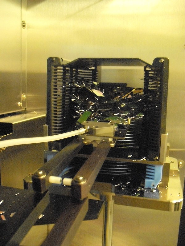
Elevator maintenance
Vacuum controller calibration
As today not many issues, able to focus and complete the tasks within 3hours.
Hopefully able to pay attention next time as well. details work come with concentration!
Metal bump as liner crack
A week start with reported product scrapped due to metal bump. And this sourced from the reason liner crack.
As our QA feedback , 2 pieces previous rework product has failed their parameters, so these 2 products need to scrap inline.
They have already inked off the affected for checking.
crack line detected after back lapping.
Defect detected 100% during AVI scan , tried to salvage with bump metal removal but did not survive in lapping step.
No Choice but to accept, and start to write report for it.
Carbon brush schedule change
Ever since the issue out, we decided to change out the carbon brush routinely.
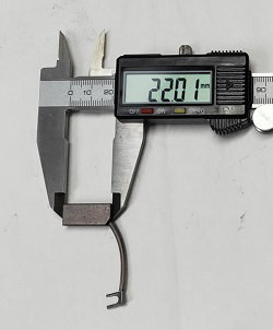
**Change carbon brush. Return used part to supervisor**
tag_img_MF-00030372_end
Clean and vacuum out commutator from traces of carbon dust.
There is some spec to take:
Measure Armature resistance (A1 - A2)
**[Spec: 6 - 10 OHMS]**
Measure Field resistance (E1 - E2):
**[Spec: 1.0 K - 3.0K OHMS]**
Also need to cascade to the rest of team for deployment.
Temple smacked for donation money
This morning my brother sent me photos that bringing bad news.
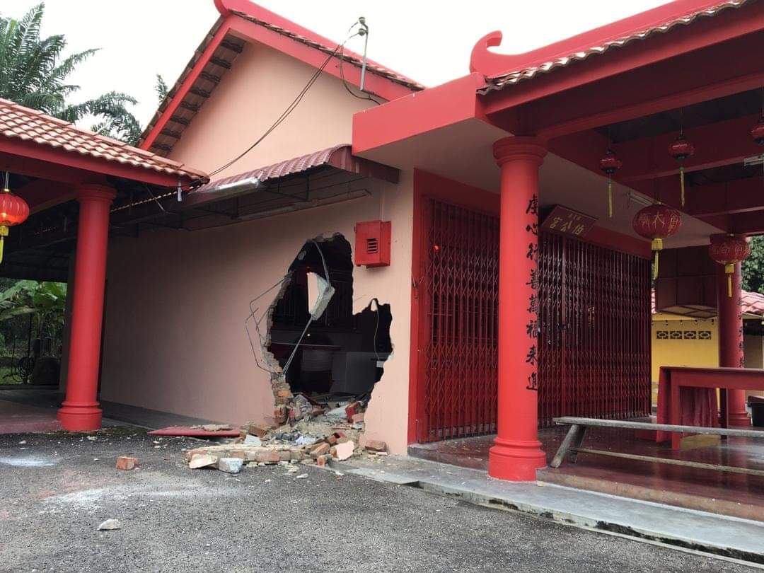
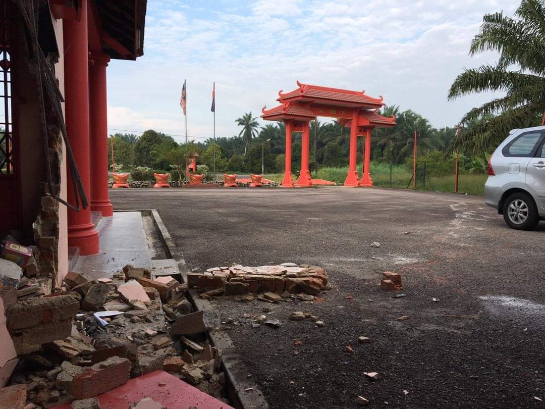
The temple that our parents always went get smacked ! the thief in order to steal the donation money from the donation box, they even smash the building off just to get the money !
This is sickening! After so many years established in a peaceful village, now encountered this kind of things after centuries !
Am not sure whether this time round pandemic give a hard hit to many people on the ground and causing them tried very method to get money !
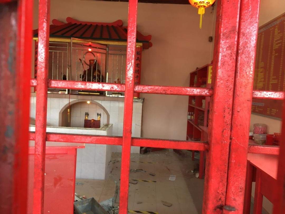
Internal view of the temple, was just a mess after these thiefs visit.
Sickening thief never let go any chances or corner to find any single money be it a coin or small note!
I have no idea what tool they use the hack the wall. And I think the temple management wont be stupid to leave big sum of money in the temple over night.
Spend so much effort , but mostly can get some RM100 donation money (USD25 or less), worth the effort?
But to the temple management, to replenish the wall would cost them tens of thousand for the work !
This is insane!
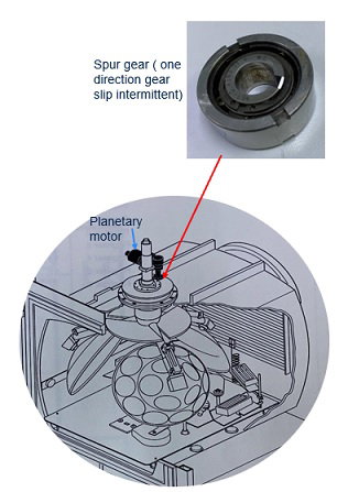
Troubleshooting for spur gear
Issue arise so have to work the troubleshooting guide for line people:
Change spur gear
Record name of EES who double check the spur bearing
Check planetary rotation for any jerking or jam. Note: Ensure planetary can only rotate one direction by hand
Check for clearance between each planetary. Adjust if necessary
Manual control to toggle planetary rotation “ON” and monitor planetary rotation for 1 min. Ensure each planetary does not scratch each other and chamber shield shield. Escalate to EES for troubleshooting together if failed.
Check rotor rotation (free to rotate and no knock of bearing)
Motor carbon brush change
Day couldn't be worse when week started with product scrappage.
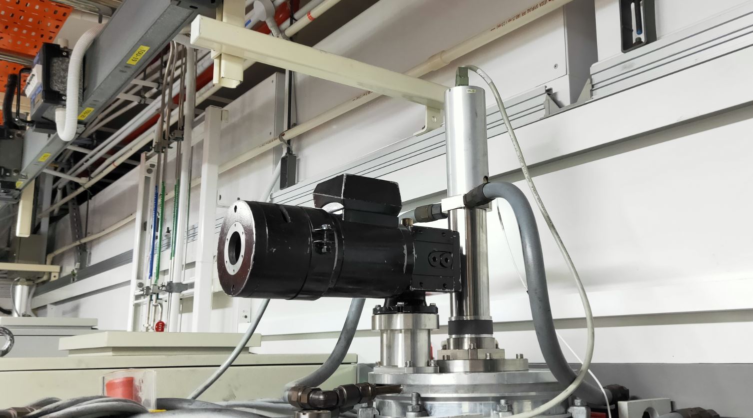
Today main actor is this motor , which is situated on top of the machine , where you have to climb up to access it.
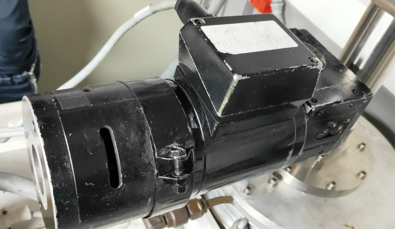
Closer look at the motor, you will have to loosen the nut screw to access to carbon brush area.
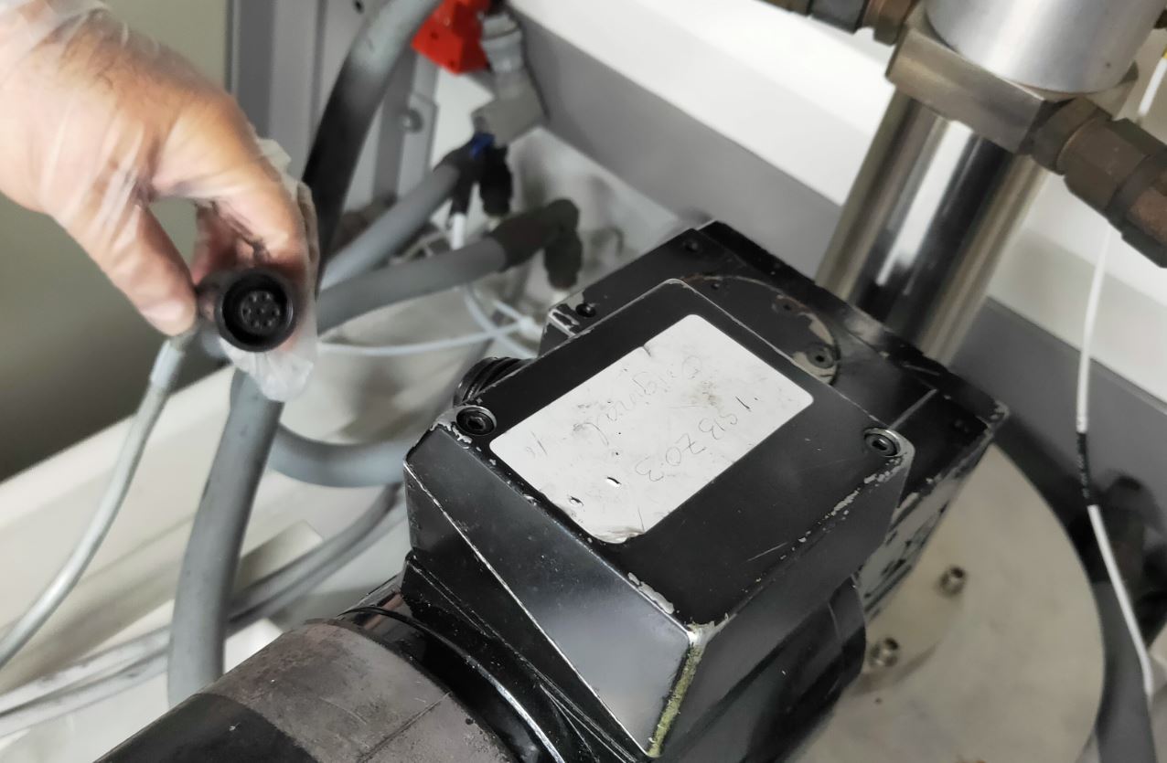
First before hand, definitely is to remove away the power cord.
Then at the external part of the motor, loosen the locking screw and move to get the carbon brush out.
While this carbon brush looks very small, it determine how the planetery motor spin. Too short then it will give alarm and fault out. Best to have periodical change out of this part, rather than waiting it to fail.
Robot blade servicing in semicon industry
I work as technician in a Singapore semiconductor factory. Here I share my working life as technician.
Friday was not a good day, because there is a scheduled maintenance on one of the machine. A tough one- that is to change the robot blade bearing.
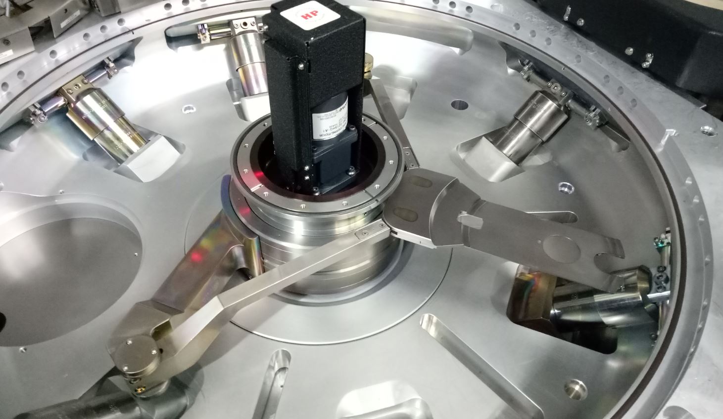
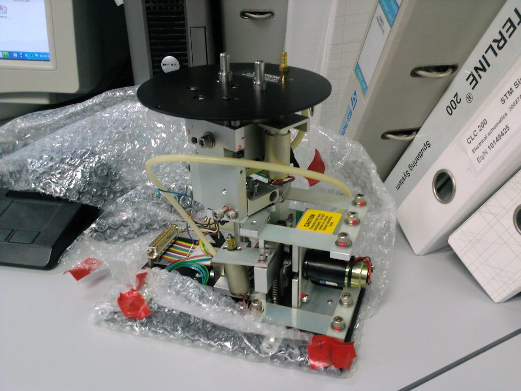
A robot blade is looks like this:
It's basically transferring the wafers from one chamber to another or to loadlock to transfer out.
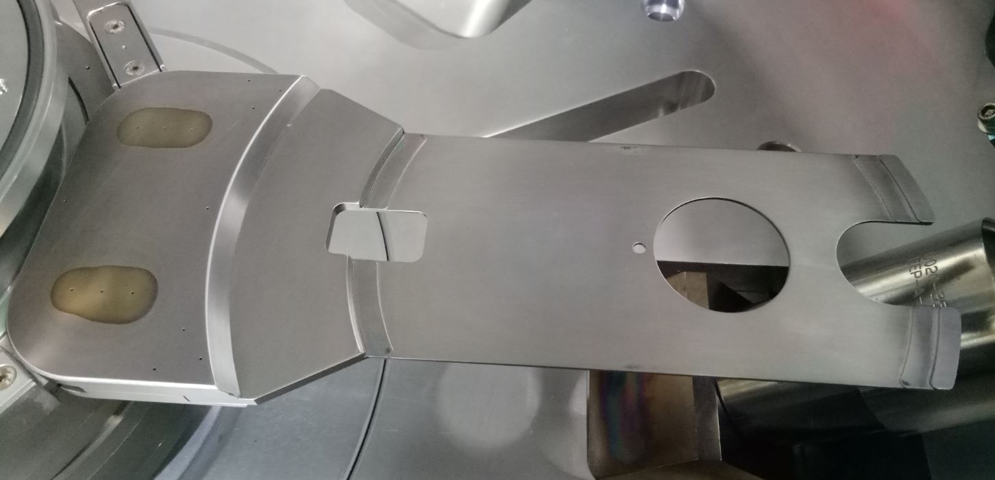
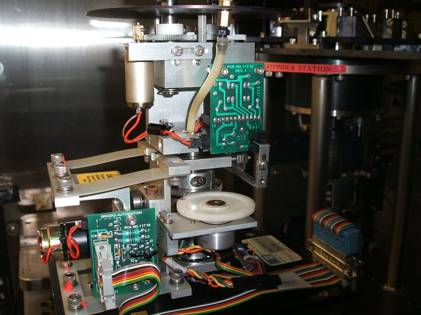
So the main character is this robot blade:
You will have to lock up the robot movement first, then dismantle from assembly using the jig.
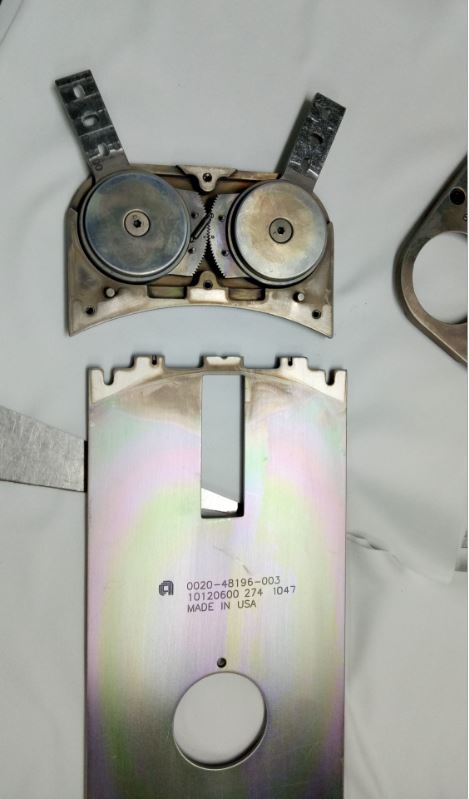
A dismantled robot blade look like this. After taking out the cover, then you see inside there is bearing for movement rotation. And a small spring to latch both gear together.
The job of changing the bearing itself is not that tough, but the aftermath is the key toughness.
You will have to calibrate and teach the robot the correct setting into the machine configuration.
You have to use checking tools to make sure the robot blade is levelled always and not tilted up or down to scratch the production wafers. Once scratches then there gone our annual bonus..
So the best strategy is getting another technician over to help you command the robot, and one is focus in checking the robot alignment. Better to be safe than sorry !
Today really a drama day for Malaysian Politic. Anwar claimed that he secure the majority of Senators' support and able to form new government. But Agong was still in hospital so unable to meet him. So , tonight sure a lot of price tags flying here and there. Frog is pricey in new era !
Buying property in Johor Bahru
Over the weekend, I came across this youtube video by a property investor who quite famous in Iskandar Malaysia/ JB area.
https://www.youtube.com/watch?v=d-Oagjx9tLg
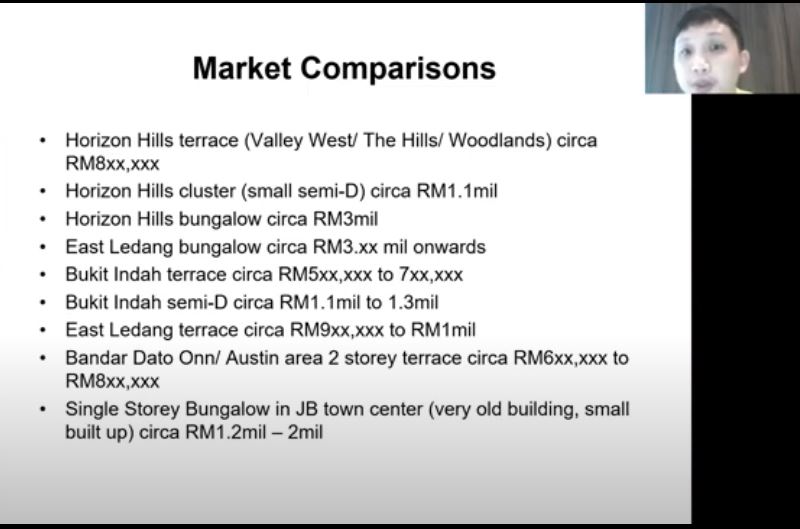
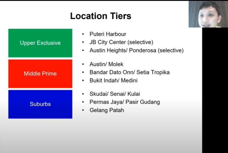
As watching through the video, I find these 2 slides to be among the best value for me to keep as referrence.
And this slide I also find useful, realise the place I always hang out is only middle prime, i should spend more time to go upper exclusive and get a feel how much price index is there. Maybe I could get some hint or clue then place my first investment there.
As much as property is concerned, definitely need to think of the connectivity prospect. Still need to survey more about it.
Belljar coil
Continue my previous journey of writing semicon life.
Today i wanna talk about the belljar coil.
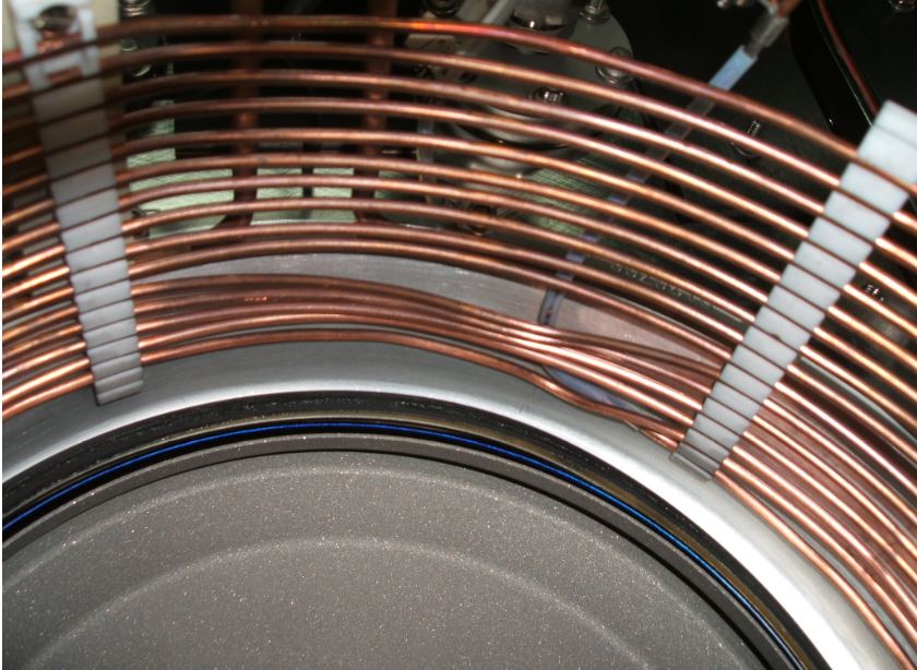
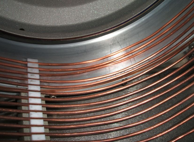
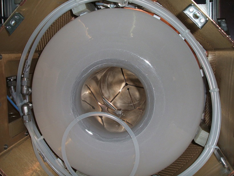
This copper line that circulated around the belljar, is functioned to heat up the belljar and make it to etch the oxide more evenly.
If the belljar coil is misaligned like in the photo, especially after the PM after the belljar installation. Then we will encounter the etch rate cannot achieve issue.
You also need to have a scanner eye to be able to detect the coils is shorted together like above photo. This also will cause that area etch rate high , but other area will lower and uneven.
But this also require some experience in installing the belljar, as it's firmly and tightly circulate the belljar, very hard not touching each other and short it.
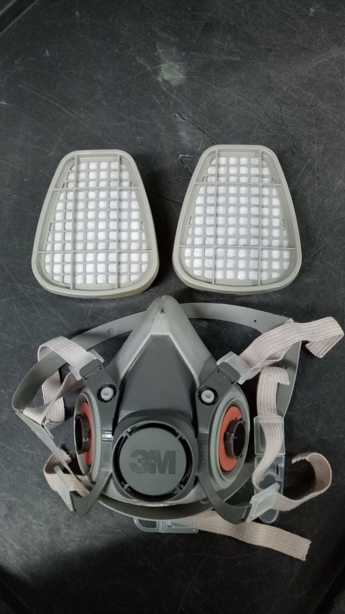
PPE for semicon factory
Due to the environment we are working, some area is working with some toxic gases. So we have to be very careful when handling the machine.
First foremost is respirator, and the cartridge , which is supposed to change every 3 month if follow the rules strictly.
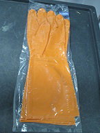
Next is the glove, if you handle with chemical, becareful when wear it all the time.
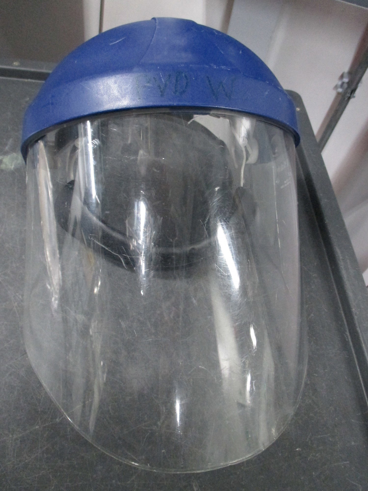
Faceshield also one of the important PPE to be worn , mainly is to prevent splashing of chemical and or gas.
Last but not least is the apron. then all these combine to be a full set.
Fish Soup as lunch
Nearby my house there is a restaurant that sell good fish related food.
You can order their food noodle
Or fish porridge
Today the weather a bit cold, so we decided to take both hot meal.
The fish noodle soup
Also the fish porridge
As their fish slices is very very fresh, this make their soup very very sweet with freshness.
And the special part is , their food served in a small hot pot, so whenever you eat, food is just as hot as it was cooked. Super good to eat during cold days
Restaurant address as below, strongly recommend to you if you were passby this area. Jalan Bestari 3/2 Taman Nusa Bestari Johor Bahru, 81200 Johor Malaysia
Target Punch through and scrap
I work as technician in a Singapore semiconductor factory. Here I share my working life as technician.
Lately we have another tool issue, that is deposition uniformity out.
So upon investigation, we suspect there is some other foreign material in the deposition. We decided to vent the chamber and check.
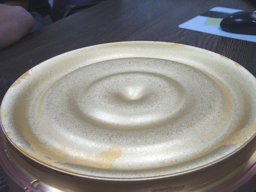
The target upon open out, looks like this, wonder if you observe any abnormality?
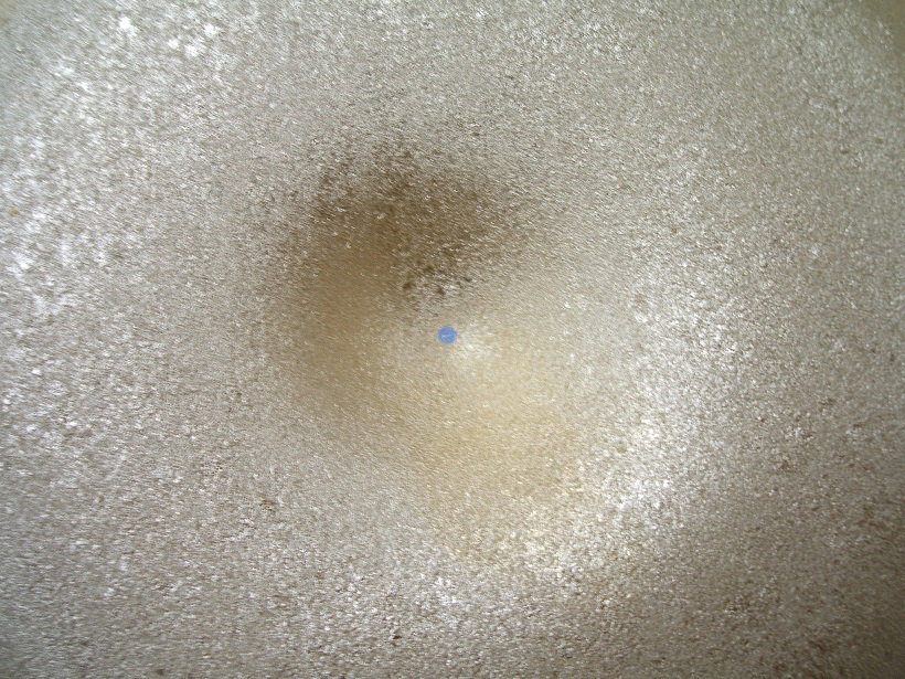
Maybe another angle for your referrence to check.
You observe the center of it is a valley shape right?
Yes the problem is the center of target was "eaten" too much too deep, until it finished off all the original material, and expose out the backing plate material. This is different from what we supposed to deposit already.
Product will be scrapped if wrong material is used. Too bad , in this case, all the products wrongly deposited will be all called back and scrapped. Sigh..
Target debonded
I work as technician in a Singapore semiconductor factory. Here I share my working life as technician.
Last week , a tool in our production line ran into problem , failing some parameters constantly.
So we decided to open the chamber and perform the inspection.
Found out the target (tantalum) had been debonded. From surface it looks like uneven surface. Looks like patch by patch over the target
Back of the target hardly see any abnormaliy.
Possible root cause maybe the shaft area, further investigation still on-going though.
Welcome everybody come visit my page for all technical stuff:
**https://read.cash/@technician**
Heater installation and inspection
I work as technician in a Singapore semiconductor factory. Here I share my working life as technician.
In our production line, heater plays a vital role, because only with hot temperature, the process able to take place and do the metal deposition.
So to monitor the heater performance and lifespan become important.
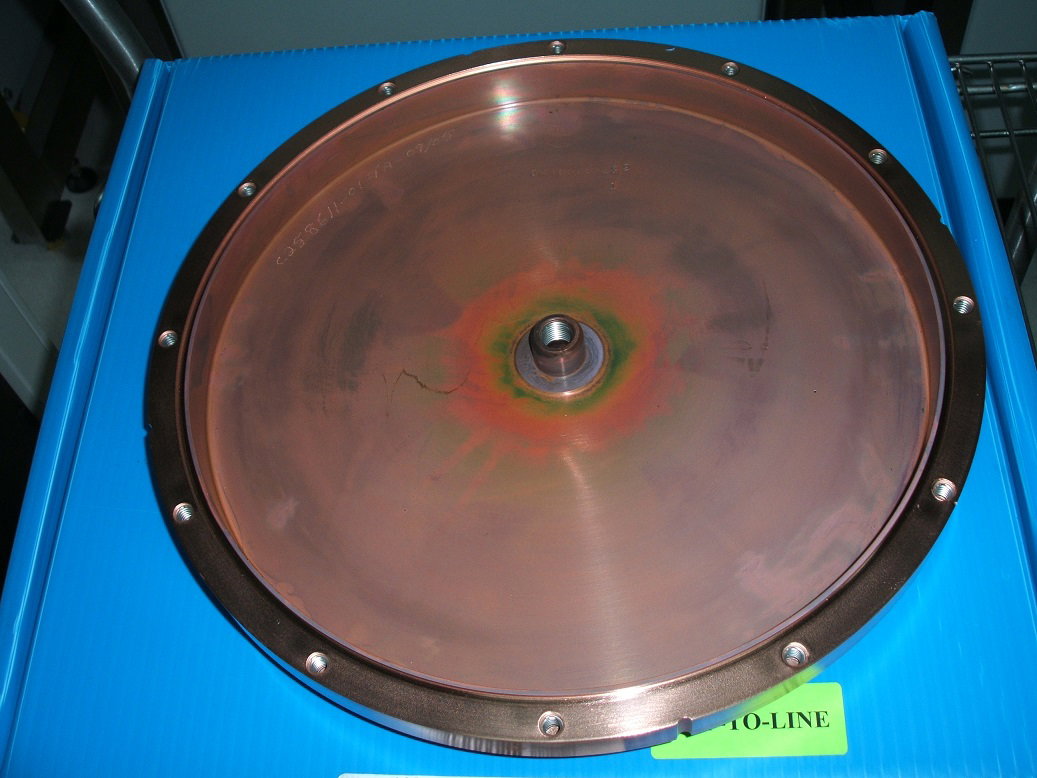
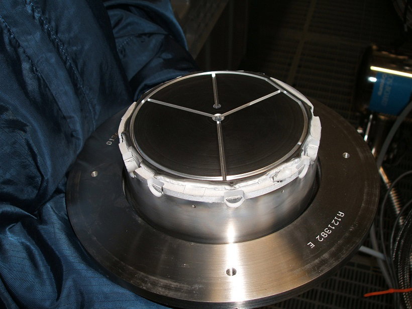
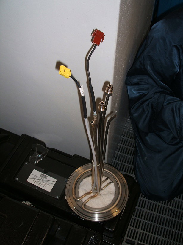
This is how it looks like for a heater.
Today we get a heater from the leader, need to install into a chamber for replacement. This is how the whole heater looks like:
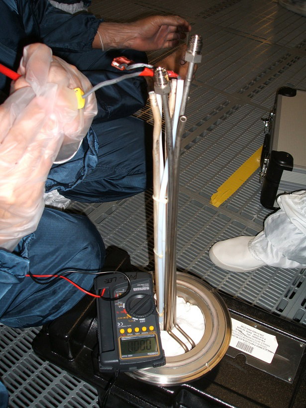
But before installing the heater into the chamber, need to double check the heater part performance. But using the multimeter, check whether the connection is short-circuit somewhere prior to installation. This is important, you do not wish to install in everything then only learn that this spare heater is faulty one, then you need to do the whole installation for over again. Waste time waste man power.
Welcome everybody come visit my page for all technical stuff:
https://read.cash/@technician
Aluminium Copper peeling
I work as technician in a Singapore semiconductor factory. Here I share my working life as technician.
The process involves the metal deposition onto the wafers, it's just matter of what target material to be deposited subject to the process need.
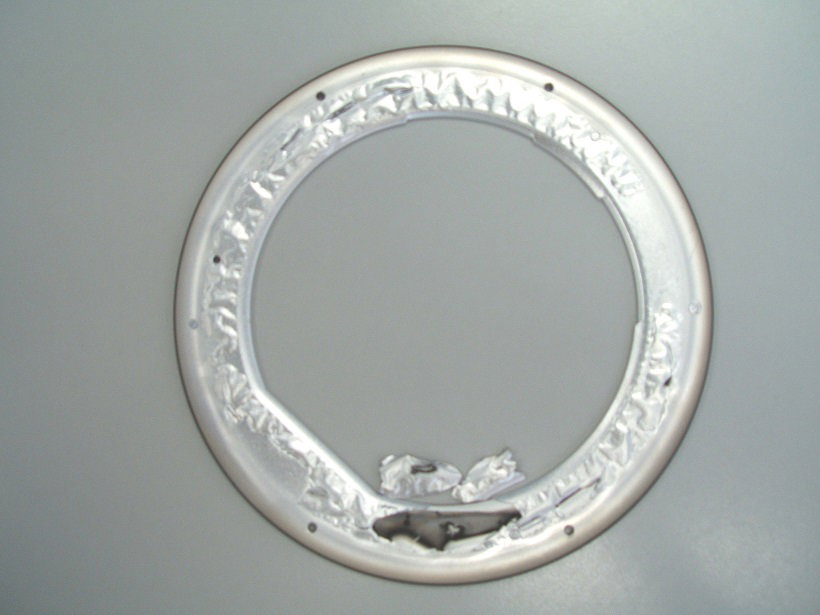
This I am going to show is Aluminium Copper (AlCu).
As you can see, the surface of the clamp ring is popping up like going to peeled out.
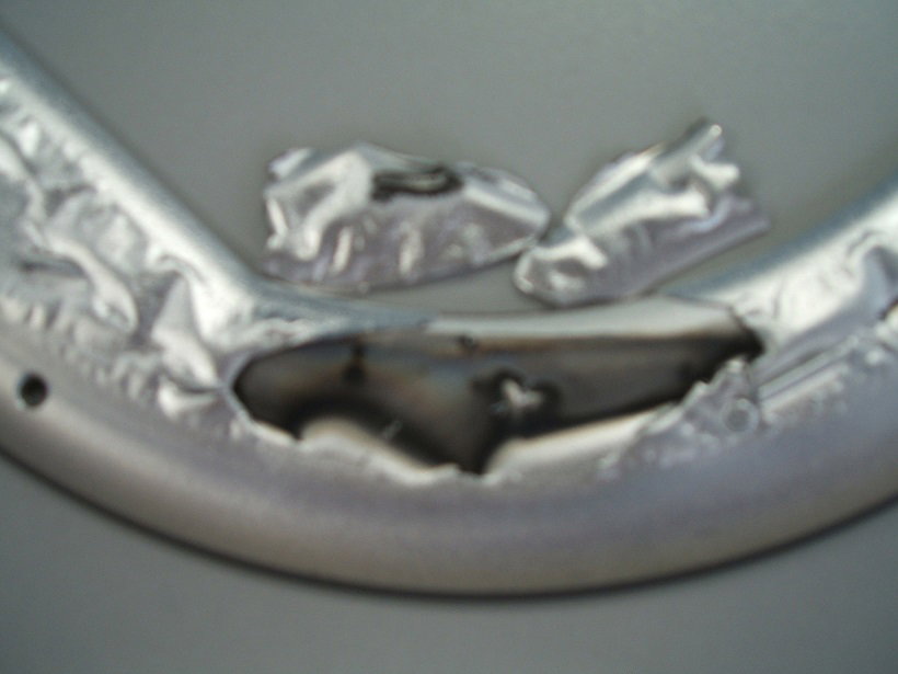
While the bottom side already have portion that already come out.
Closer look at the peeling off area:
Nothing much can be done, except change out all parts, clean up all area, and make sure root cause identified and move forward for tool recovery .
Heater flatness
I work as technician in a Singapore semiconductor factory. Here I share my working life as technician.
In the chamber, heater is the most critical part, not only does hot surface makes the deposition at faster rate, but evenness of the heater to make sure the deposition of metal is equallly onto the whole wafers.
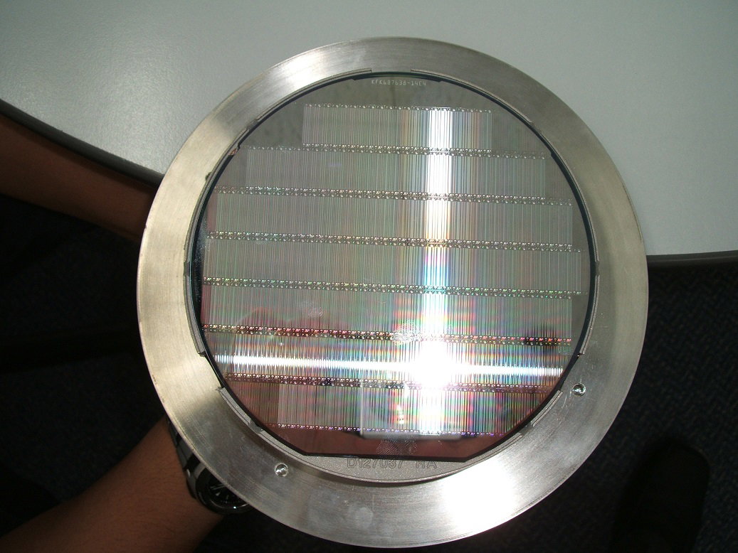
This is how it looks like , a wafer sitting on a heater.
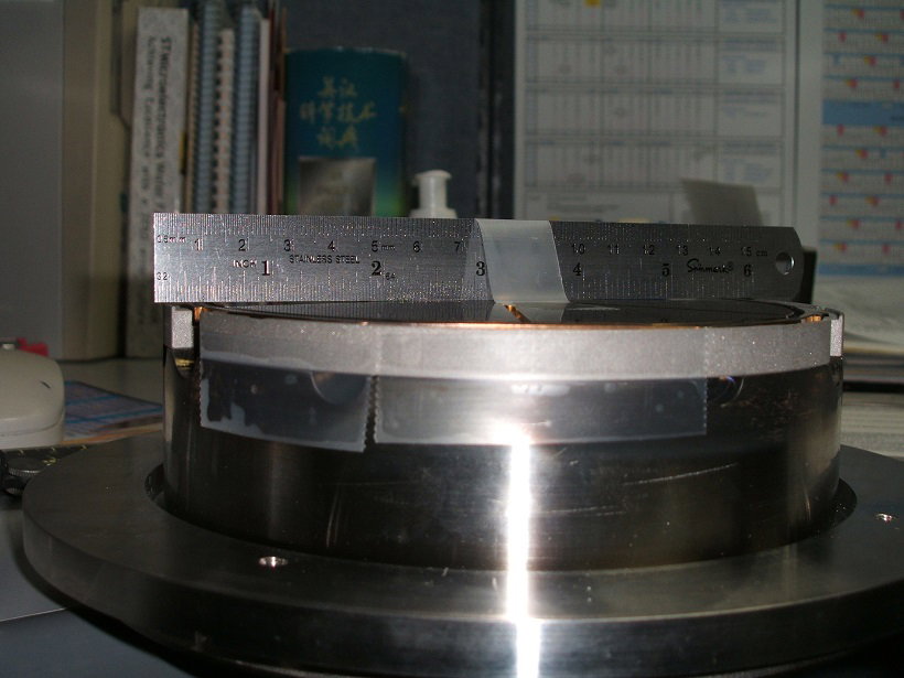
When we dismantled out the heater, rough gauge is by using a ruler, though not a good one. You will roughly get whether the surface is flat or not.
Another factor that play a part is the side groove. The screw need to install in nicely.
Another angle of the wafer holder sitting on the dismantled heater.
Top view of the heater , this is a good one , just need to polish a bit on surface with scotch bright.
Gold target lockout
I work as technician in a Singapore semiconductor factory. Here I share my working life as technician.
As our process run with precious metal, there are many security layers implemented. Not only did we need to step by step withdraw the target, we also need prevent from physical lock to the machine.
There are many different locks design we design and trial.
First we made a full metal box to cover the whole target.
But over years we found that design is not that solid and fool-proof. So we came out of simpler yet more effective way of securing like photo below:
This design is more handy but more effective in a way , easier for technician to do maintenance yet serve the purpose of securing the target.
Design still not change yet, but definitely one day we will need to relook into this matter and design better one.
Gold deposition peeling
I work as technician in a Singapore semiconductor factory. Here I share my working life as technician.
Continued yesterday topic - the gold deposition peeling off.
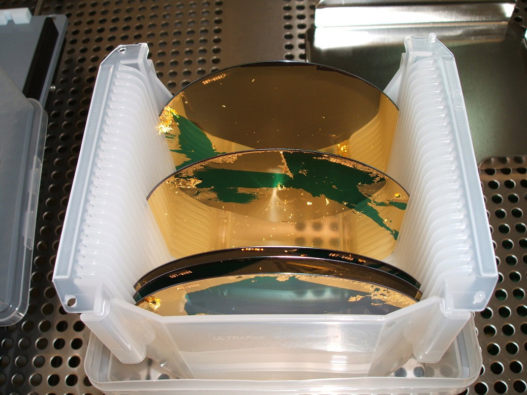
The seasoning wafers that get peeled off need to gathered and do analysis soonest possible.
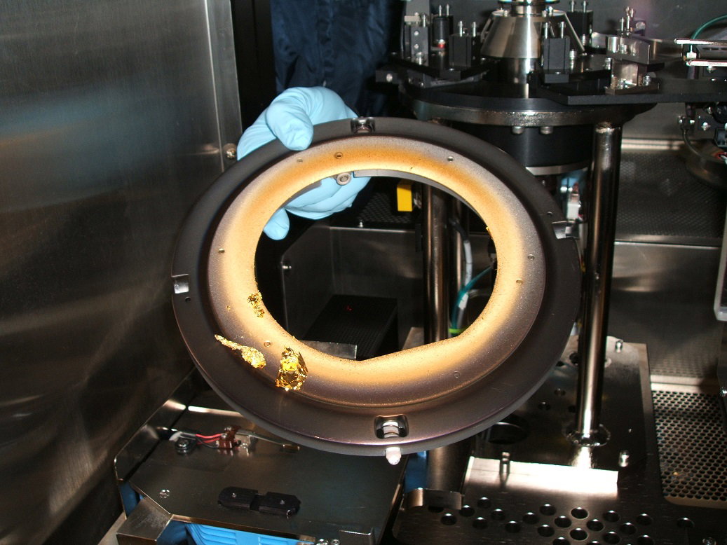
The peeling can fly off anywhere, and the most sticking could be those with contact with chamber, eg the wafer holders. All the wafer holders need to change with new assembled.
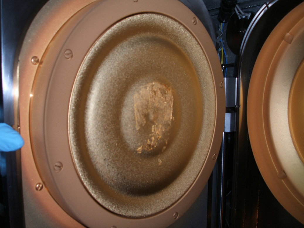
Another big problem with peeling is, you have to vent out the chamber and do the cleaning. As you can see photo below, the peeling already stick back to the target itself. If this peeling is not cleared off, the deposition will not get uniformed deposited onto the wafers and affect the film property. And next leading to wafer scrappage.
The BJ story in semicon industry
I work as technician in a Singapore semiconductor factory. Here I share my working life as technician.
In our line of semicon, we refer BJ to belljar. The function of belljar is to suck.
Suck away the oxide layer on the product (wafer) before the next step metal deposition.
But you cannot let the BJ to suck too much. Working too hard (Used too frequent) then it could explode. And you will get very "excited" to see this scene.
All BJ broken into pieces and you need to clean the shit.
After explosion, you will expose the chamber to the atmosphere, And you get even more excitement of the suction. All dusts and debris get into the chamber and could harm to the pump and choke it.
Broken BJ at the welding point, a common weak point.
Another weak point is at the side, where this is more contributed by BJ handling. BJ is not treated gently then it broke during transportation.
When BJ broke, investigation need to take place and analyse the weak point and questions why it broke. So as to prevent similar problem arise again.
Excited to know more about the BJ? Hope you enjoy the series of BJ. Thumb up if you enjoy reading this. Thanks
Metal peeling
I work as technician in a Singapore semiconductor factory. Here I share my working life as technician.
Today I wanna talk about process related issue in our line. We called it in layman term peeling. Meaning the metal which supposed to deposit onto the product is not sticked to the wafer but peeling off when it comes out from machine.
First let you to see mild cases:
As you can see sides have got minor peeling.
This is more serious. top side is peeling off very much.
As the process is deposit a layer of precious metal. The peeling piece also need to be collected back for claiming purposes.
normally the peeling will be happening in whole batch especially after target change PM , all the seasoning wafers will be peeling some severe, some less.
This peeling is mostly due to the stress applies during the deposition. Uneven pressure or stress could react and interfere the deposition rate onto the products.
This scenario we hope to avoid , as not only need to settle the machine problem, but also the precious metal debris collection - super tedious with many paperwork to followup as each piece could cause few hundred to thousand for reclaim...
Chillers for semicon
I work as technician in a Singapore semiconductor factory. Here I share my working life as technician.
There are several types of chillers in use in our plant.
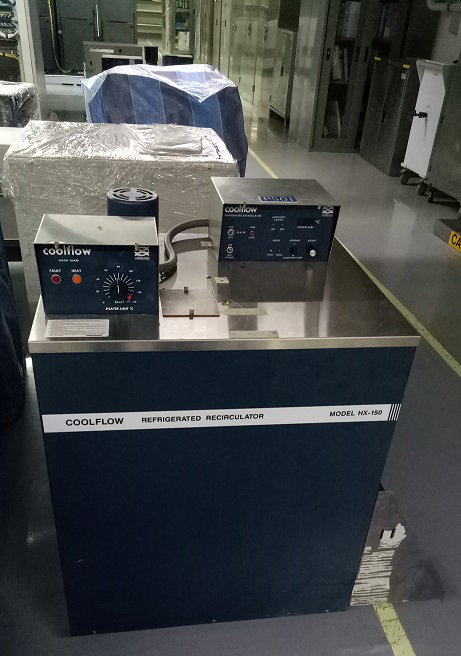
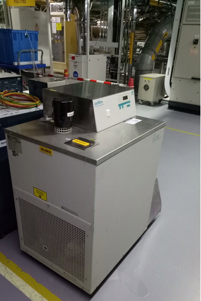
The most popular is this blue color type, called Neslab Chiller
It has a upgraded version, also called Neslab but in white color, so we call it Neslab White. Just to differentiate the old and newer model:
Both Neslabs models is already obsolete, where the maker of the chillers not supporting the sparepart. So the market repairer need to source it somewhere and cause the repair cost at high side.
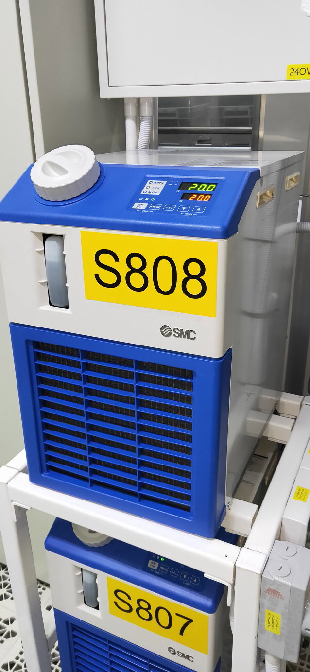
So actually there are few replacement for the obsolete issue, that is SMC chiller replacement. Its pump function very strong and temperature maintain is good. Just the problem in it is not integrate into machine alarm.
Talking about the neslab, the frequent failure in it is cant maintain at temperature setpoint, then you need to topup the refrigerant gas and make it chill down.
Hope you like my article about semicon industry in Singapore, and give me a thumb up if you find it useful and interesting. Thanks.
Small ADAM for communication
I work as technician in a Singapore semiconductor factory. Here I share my working life as technician.
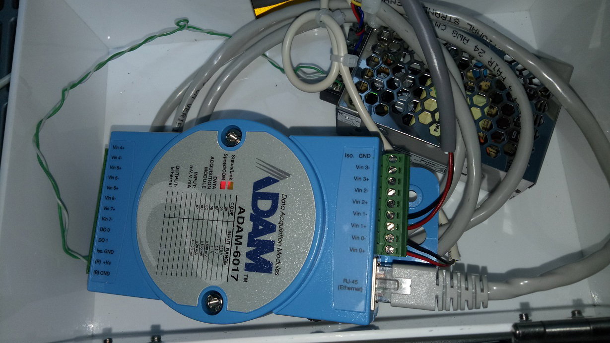
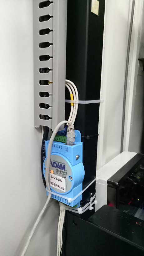
Small ADAM is used when you know there are limited channels that you going to have for a tool. With only 8 channels configurable, you'd better make sure you do not need to add more channels in near future to prevent channels not enough.
The only good thing about Small ADAM only is its size is handy , so simply a box able to fit it and work fine.
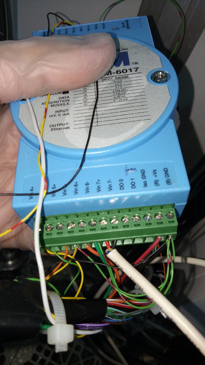
But small ADAM is bringing more problem than the benefit it brings , the connection simply just unfriendly. 4 channels at one side, and 4 others at the other side.
The cable tidiness is more difficult to achieve.
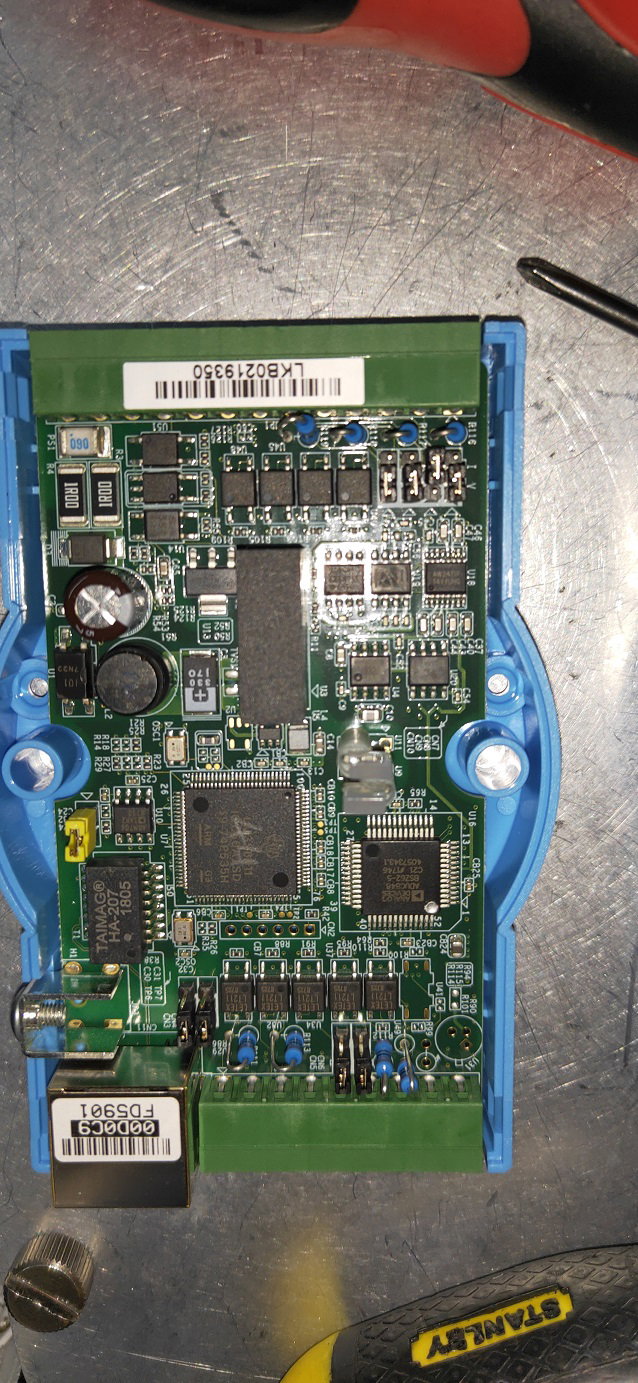
Small ADAM also having another significant drawback, older version you will have to open up the cover to toggle the settings, eg from current input to voltage input and vice versa.
Though the newer version have improvement over this weakness, they put it behind the cover. Yet consider the messiness of cable, in order to access this dip switch at the behind, also take some effort in it.
ADAM configuration
I work as technician in a Singapore semiconductor factory. Here I share my working life as technician.
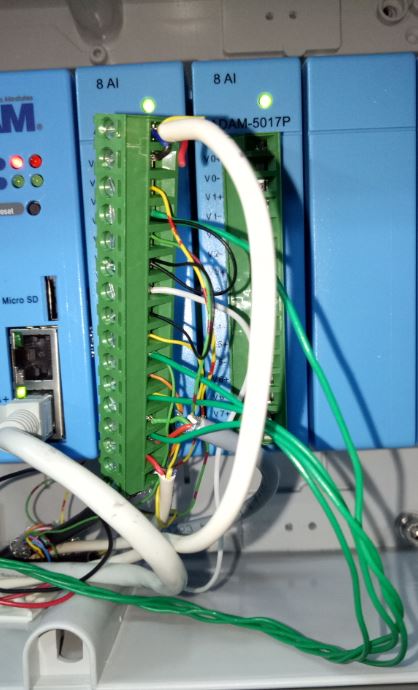
Continue the topic on ADAM controller, as you can see from the photo below, it can be connected to many different function sensors. Just need to take note the exact channel will do.
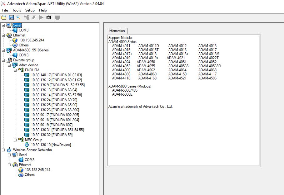
After physically connected to the ADAM, you need to go ADAM @net software to do the configuration of channels.
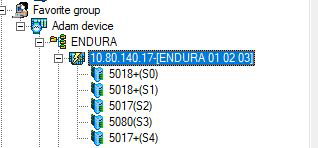
For different small card, also of different function, 5017 can take voltage and current. 5018 to take temperature.
For 5018, temperature can measure up to 1370C , but maybe your TC could spoilt before it take its reading..
Then take note the Modbus , to configure the connection to server.
While 5017 card, you can set whatever range your sensor working, eg 4-20mA for water flow sensor, +-10V for temperature. 0-10V for pressure transducer reading.
Wafer Holder Assembly
I work as technician in a Singapore semiconductor factory. Here I share my working life as technician.
The product -wafers need to transfer from the cassette to the machine , and 1 by 1 mounted onto wafer holder and transfer into chambers to do the deposition.
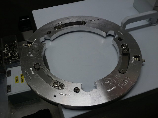
This is the wafer holder housing, as you can see 2 ceramic pins at the side to hold the assembly to machine seal ring
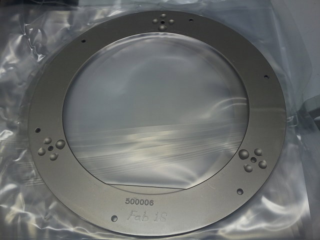
This is the clamp ring, wafer sit on this piece.
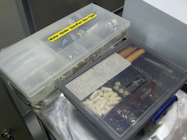
The full set of PM kitting for wafer holder preventive maintenance (PM): 5S is always emphasized in the work place.
the wafer holder assembly area, graphite stone for flatness monitor and checking.
As it's critical for the wafer holder assembly work to be done properly. Most of the time need to dedicate 1 person to fully concentrate the work and record down the part number and serial number for tracking purpose.
Belljar & issues
I work as technician in a Singapore semiconductor factory. Here I share my working life as technician.
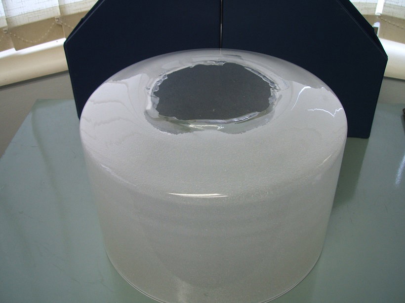
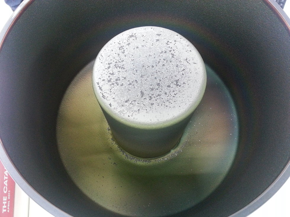
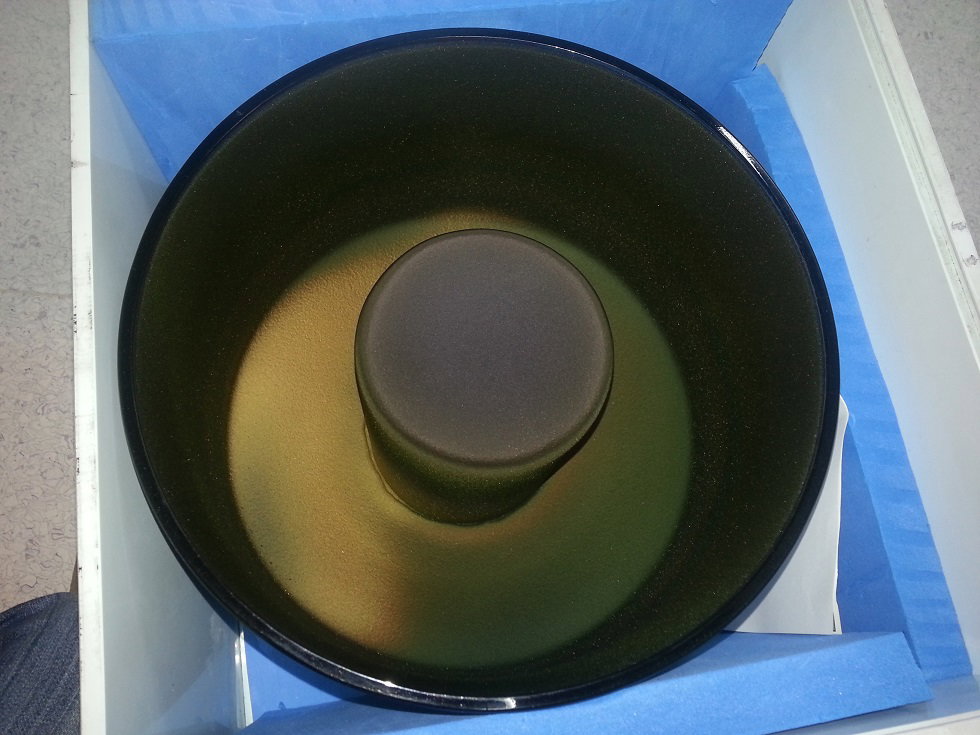
A belljar is made of quartz, and its function is to etch away the oxide layer of the wafers, before proceed to next step- metal deposition.
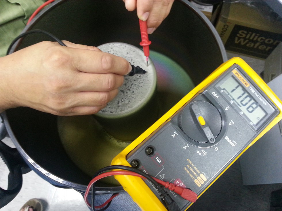
But one common problem with belljar is due to man made mistake- that is running with wrong wafers and get etched away into Belljar, so the belljar is contaminated with metal coating.
Using multimeter ad can see the metal coating causing conductivity. Belljar need to dismantled and send out for cleaning.
Below photo can see heavily coated with copper. become conductive.
Another issue with it is over use of belljar, or stress in weak point , the joint area. Below photo is broke at welding point and causing long machine long down time as need to clean the debris.
As belljar made of quartz , dimension is very critical. And also costly to make one.
Stay tune for more Singapore Semiconductor Technology !
Transfer Robot Arm
I work as technician in a Singapore semiconductor factory. Here I share my working life as technician.
To move the product from the cassette into machine and run processing - deposit few layers of different metals onto the product wafers. The machine need a robot arm.
This is how the robot arm looks like:
At first glance , it really looks like a Lego toy. But in actual fact, our this machine since it's pretty old technology (history up to 30+ years). We are using this kind of robot arm.
This is how it looks in the machine.
This is how it looks, when the robot arm clashed with the products. Could due to sensor faulty , could due to cassette platform moving, then robot arm sudden extend out of control.
The robot blade bented badly in this case, view from different angle. This must be a bad day as investigation reports will need to prepare before tomorrow production meeting. Sad. Lots of questions will be thrown by all parties...
Wafer thickness measurement tool
In Semicon especially in Singapore wafer fab which demand a high quality output, Every product will need to go tru some sampling check. Meaning to random check whether process is under control eg if we wants the metal deposition to be certain thickness, the machine cannot deposit more or less to certain percentage, eg plus minus 5%.
Thicker or thinner of the metal will affect the product performance.
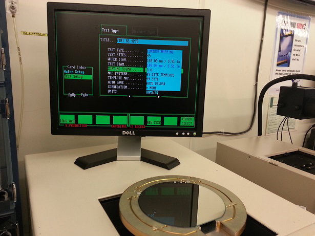
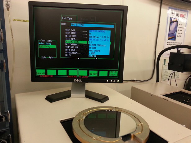
So we use the RS machine to sampling check the thickness.
Measurement tool looks like this:
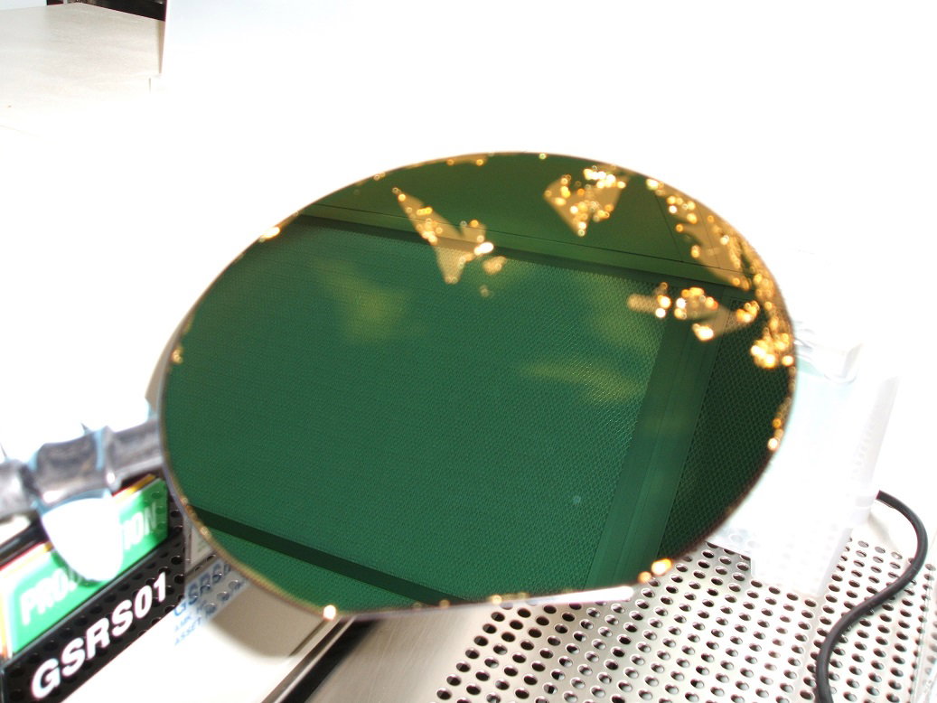
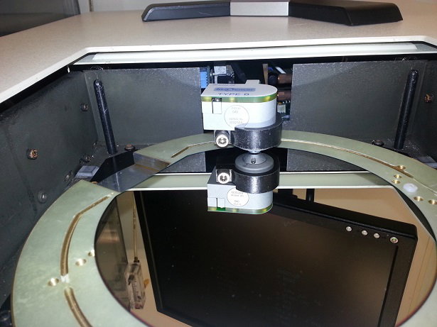
and the probe on the wafer in closer look.
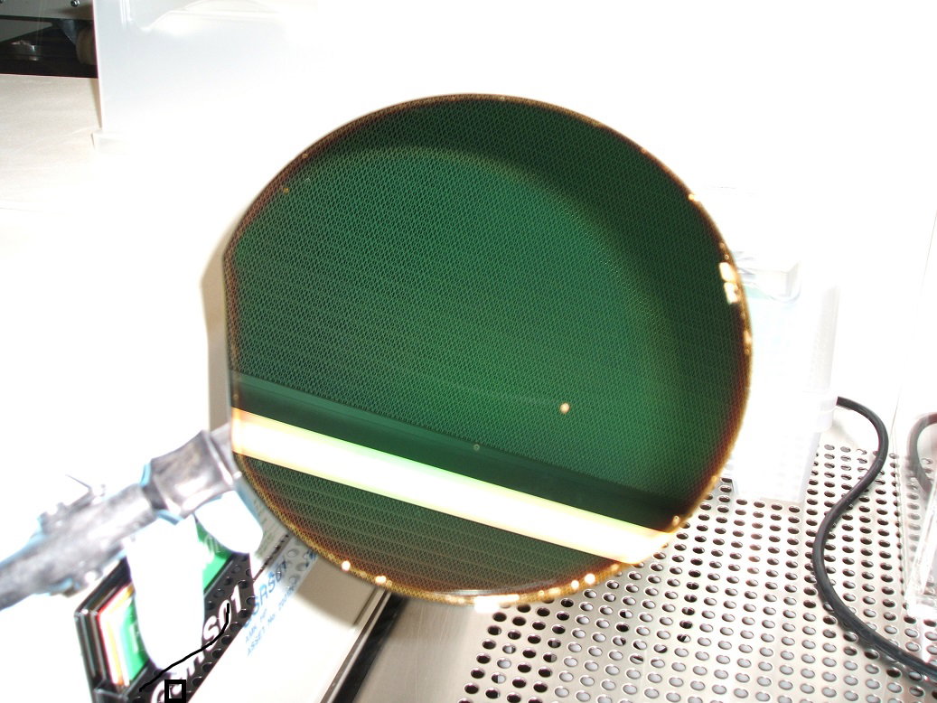
So we look at the mean for average thickness in all areas of measurement, so some we take 49 points measurement, some 5 points, some 17 points
And the results also can be displayed in contour map. In this photo , thickness slanted one sided..
Also can choose 3D dimension map display to have better illusion how the thickness , whether slant one side , thick at center or whatsoever.
Semicon - magnet and target
Today I wanna continue talk about the semicon stuff in Singapore.
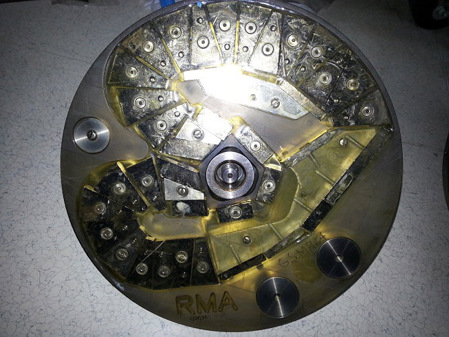
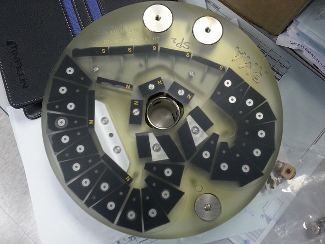
Picture below is a magnet, a super strong magnet plotted polarity in order, so the magnetic field is very strong, dont get near your phone with it , or else will stick to it and hard to dispatch.
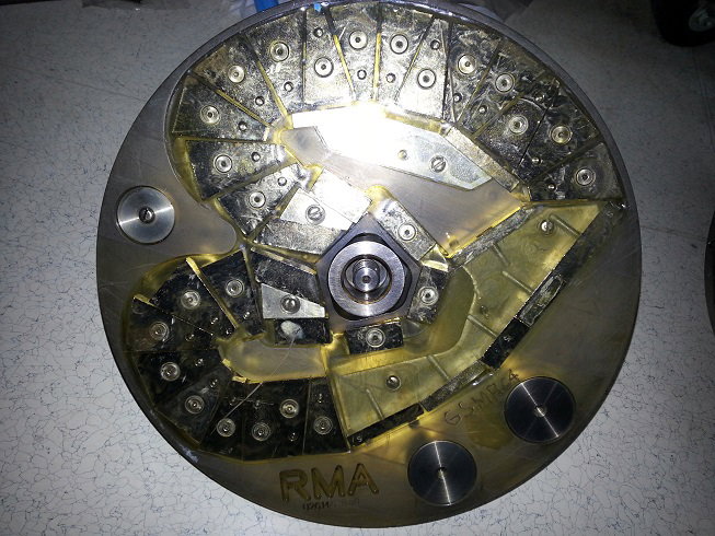
This is called the RMA type magnet.
Two versions of it , one is silver color and newer design is black color.
The use of magnet is attracting the ionized metal , to be bombarded into the product- wafer and do the deposition.
And magnet magnetic field is critical in determining the lifespan of the metal target. We have to take note the lowest point on the target in order not to punch tru and deposit different metal to the products.
And this is another type -RMM type, will be used for another type of target, but this RMM is much more expensive because the magnetic stripe is bented another structure.
Technician's life
Hello world, I am new to this space. and am introduced by @sitisan to write and share.
I am a technician in semiconductor sector in Singapore, as I explore , not many articles about this area here in this space. So I think I would like to share more in this area.
Maybe not many people know that, Singapore also one of the countries with strong semicon fundamental, this ensure the country to continue its edges in technology, and not rely only on service sector.
For a start, I write something about work life , something I everyday deal with- maybe useful to some others and find it interesting.
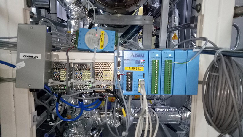
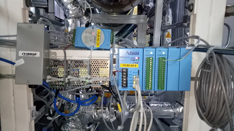
This is called ADAM , a device to connect between the machines and server. When we install new sensors to monitor something, we connect from Machine to ADAM then to the IT server and monitor.
Normally there are 2 sizes, big and small, big is preferable because the channels expandable.
And below is a normal sensor that connect with a power supply. Output from this sensor is linked to the ADAM device.
I will continue to share our Singapore's semicon technology for daily machine monitoring . Subscribe me to know more update, stay tuned !